CN/EN
 Search


Source:新声半导体 Author:新声半导体 Time:2024-05-27
Packaging technology is crucial in the semiconductor industry, as it not only protects the chips but also provides electrical connections and thermal pathways. Categorized by different packaging forms and application fields, semiconductor packaging technologies mainly include:
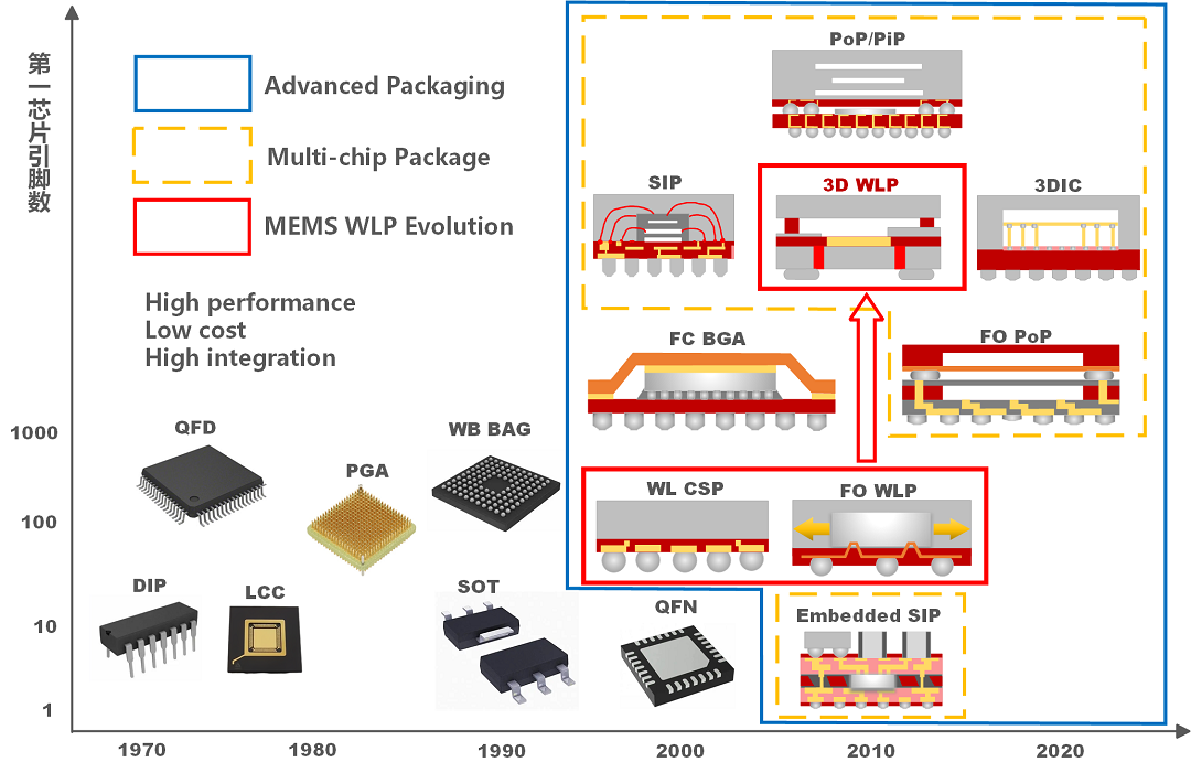
Figure 1. Packaging process evolution
Distinct from conventional chip packaging methods, Wafer Level Packaging (WLP) technology involves encapsulating and testing the entire wafer before cutting the packaged wafer into individual chips. Among all packaging forms, WLP is the only method that does not increase the area on the wafer base. This approach enhances production efficiency, reduces costs, and improves performance. Additionally, WLP can achieve a packaged filter thickness between 0.2-0.3mm, significantly lower than that of CSP. With the widespread adoption of slim smartphones, especially with the large-scale promotion of folding screens, the reduction of RF device thickness has become a hard requirement, making the importance of WLP increasingly evident.
1. hrough Silicon Via(TSV)
By redistributing and rerouting interconnect lines on the surface of a chip or package, it provides more flexible and efficient electrical connections, supporting a variety of I/O configurations and the demands of high-density interconnectivity.
3. Bumping
By forming one or more tiny metal bump structures on the I/O pads of a chip, it achieves an efficient and reliable electrical interconnection between the chip and the packaging substrate or other chips.
4. Wafer Bonding
Utilizing the principles of electrolysis to deposit a layer of metal or alloy coating on the surface of a conductive object. In WLP technology, plating is involved in the metal filling of TSVs, the formation of bumps, and the fabrication of RDLs.
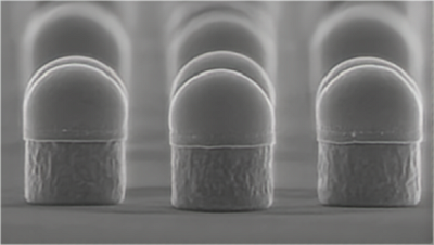
BAW filters are radio frequency MEMS devices with a three-dimensional mechanical structure (vibrating resonator units), which require a stable external environment to operate effectively. This characteristic means that the packaging of BAW filters differs significantly from traditional IC packaging and involves a more complex process. While IC packaging is planar and two-dimensional, wafer-level packaging processes such as WLCSP and FO-WLP are designed to integrate more I/O pins; BAW filter packaging, on the other hand, is three-dimensional. Beyond the pins, it is crucial to provide a sealed cavity that allows the resonator to vibrate freely in a stable environment. Therefore, BAW filters require a "3D WLP" approach.
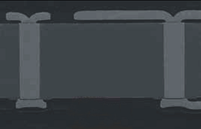
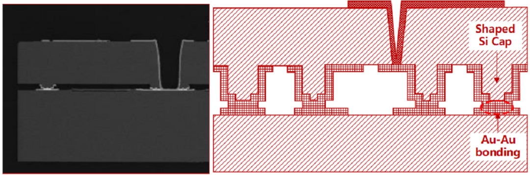
Avago's FBAR technology——Microcap achieved WLP around 2003, and laid out core technology patents, the essence of which is the shaped silicon cap and gold bonding (US8232845B2). At that time, the wafer-level packaging technology for MEMS was not yet perfected, and traditional SAW filters were still using the old ceramic housing and gold wire bonding packaging methods. Avago opted for the relatively mature Metal Diffusion packaging, using gold as the material. Avago's Microcap technical core includes TSVs constructed on the Cap Wafer, silicon bumps and rings that form the cavity, and Au Gaskets structures for bonding and electrical connection. By the rational combination of TSVs and silicon bumps, effective electrical interconnection is achieved while ensuring sealing.
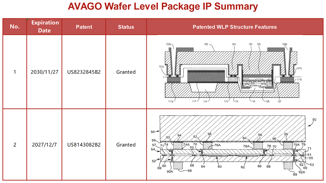
Figure 2. Avago's wafer-level package patent
Avago's unique WLP technology, Microcap, has been instrumental in the large-scale commercialization of FBAR over the subsequent 20 years. This all-silicon approach has greatly facilitated back-end packaging, ensuring that Avago can achieve higher density integration in module solutions. A 2019 research report from Yole shows that Avago integrated 19 FBAR filters in a high-frequency transmit module (measuring 7.22×6.23mm with a thickness of 0.76mm), with the area of each individual filter being only half of 1mm².
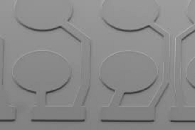
Qorvo's adoption of a double-layer dry film scheme in WLP technology is one of its distinctive features. The first layer of dry film primarily serves to construct the sidewalls of the cavity, ensuring the stability of the internal structure; the second layer of dry film acts like a roof, capping the top to form a complete packaging structure, providing protection for the internal devices. Electrical interconnects utilize an advanced copper pillar technology, which forms vertical interconnects directly on the wafer, significantly enhancing integration.
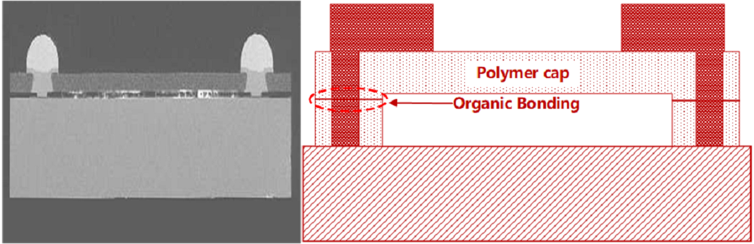
Figure 4. Qorvo: Polymer Cap + Organic Bonding
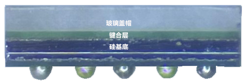
Newsonic:Raw Si Cap + Organic Bonding
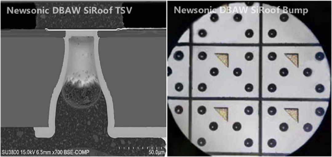
Newsonic launched its original D-BAW product series with the SiRoof packaging solution in 2021. The product features a raw silicon cap (Raw Si Cap) combined with organic dry film bonding (Organic Bonding), and Newsonic has laid out core technology patents in the United States and China, US20220103147A1 and CN113556098B, respectively. In the SiRoof design, the layout of TSVs differs from conventional WLP practices by placing the electrically interconnected TSVs on one side of the device, not on the cap side, This design means that the current path does not need to cross the bonding interface, effectively avoiding potential reliability issues caused by residual stresses in the bonding interface, the reliability level is consistent with Avago's, significantly enhancing the product's stability and durability. Compared to the Microcap, which involves multiple photomasks and complex processing steps, Newsonic's SiRoof wafer requires only one photomask, akin to a roof (Roof) covering the walls formed by the organic bonding layer, overall shortening the manufacturing cycle and reducing costs.
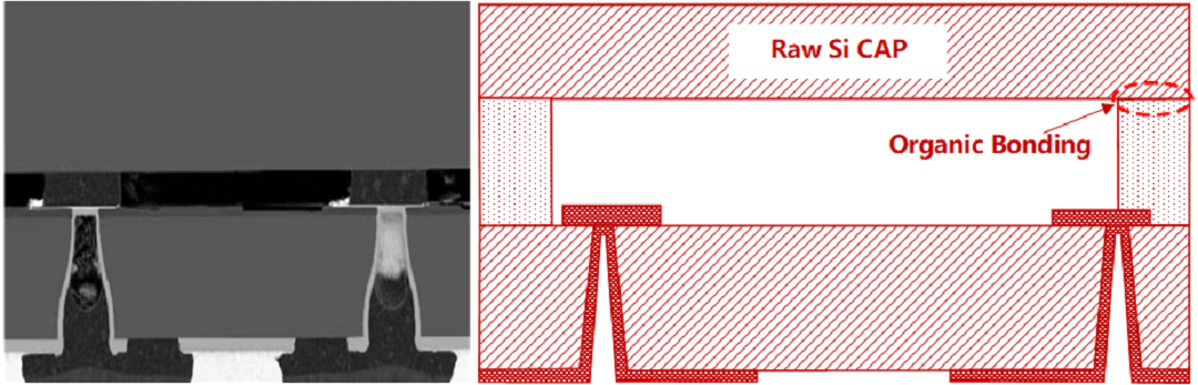
Figure 6. Newsonic’s Double-sided Processed technology: Raw Si Cap + Organic Bonding
How did SiRoof born?
As is well known, the desire for imagery is a thriving need for all of humanity, and people's lives have been completely transformed by mobile phone cameras. In the 1990s, mobile phone photography technology began to gradually develop and rapidly spread, followed by a sharp increase in the number and performance demands of smartphone camera sensors.

Figure 7.Netizens jokingly refer to modern camera modules as "mahjong tiles."

Figure 8. Modern TSV-based packaging of CIS WLP [6]
Interestingly, BAW WLP also has similar needs to reduce electrical interconnect parasitics, ensure reliability and sealing, and minimize size. Newsonic sought to collaborate with a leading manufacturer of CIS WLP to attempt direct grafting of CIS WLP onto DBAW wafers. To their surprise, the process was fully compatible and achieved rapid success, resulting in the SiRoof approach. Subsequently, the two parties collaborated to overcome process challenges such as narrow bezel wafer bonding and complex dielectric etching, further enhancing reliability margins in mass production.
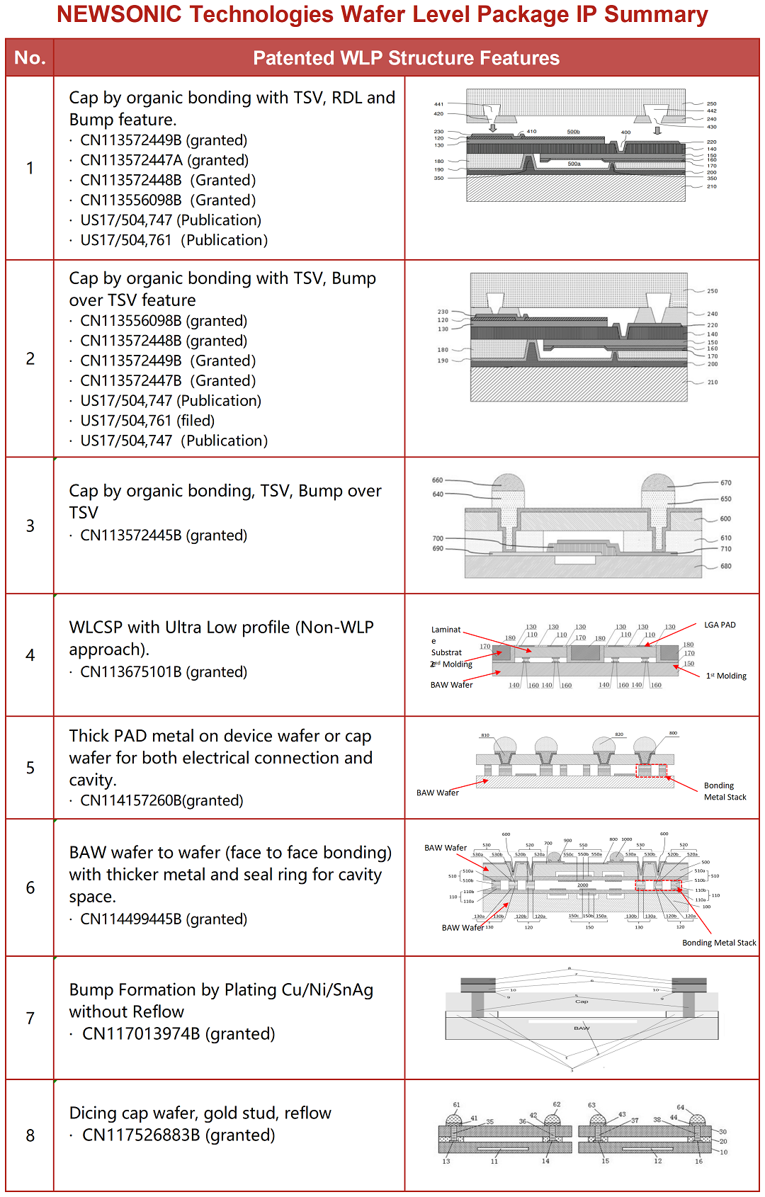
Avago, Skyworks, and Qorvo have been innovating and developing their own BAW WLP technologies independently, with Avago and Skyworks primarily based on "metal bonding" and Qorvo based on "double-layer dry film." Newsonic, on the other hand, has developed advanced and stable SiRoof technology by standing on the shoulders of CIS giants, fully integrating the advanced features of TSV in the CIS industry, the low-cost and huge capacity, and combining it with the newly developed narrow frame organic bonding and technology, flat untreated SiRoof material, to achieve its own BAW WLP.
The development of smartphones globally over the past two decades has not only changed people's lives, but also given rise to a Renaissance-like technological explosion in the "ecosystem of smartphones" industry, with the RF communication industry and the CIS industry being two of its members. In this brilliant era, we are not only shining on our own, but also borrowing the light of others.
Reference
[1] United States Patent US9219464 - Bulk Acoustic Wave (BAW) Resonator Structure Having an Electrode with a Cantilevered Portion and a Piezoelectric Layer with Multiple Dopants: https://patentimages.storage.googleapis.com/a4/25/02/1e0ba32593084f/US9219464.pdf
[2] United States Patent US8232845B2 - Packaged Device with Acoustic Resonator and Electronic Circuitry and Method of Making the Same: https://patentimages.storage.googleapis.com/8f/92/b0/ed6ee6c47a65d3/US8232845.pdf
[3] United States Patent US8143082B2 - Wafer Bonding of Micro-electro Mechanical Systems to Active Circuitry: https://patentimages.storage.googleapis.com/9d/59/fa/6486ad02d1a6c3/US8143082.pdf
[4] United States Patent US20220103147A1 - Lithium Niobate or Lithium Tantalate FBAR Structure and Fabricating Method Thereof
[5] People's Republic of China State Intellectual Property Office Invention Patent CN113556098B - Bulk Acoustic Wave Resonator Packaging Structure
[6] Ma Shuying, Wang Jiao, Liu Yi, et al. A Brief Analysis of CMOS Image Sensor Wafer-Level Packaging Technology [J]. Electronics & Packaging, 2021, 21(10): 100108
Address:Room 801, Building 3, 136 Zhongkang Road, NEXT Park, Futian District, Shenzhen
Phone No.:0755-86963703
Email:official_accounts@newsonictech.com
